Semiconductor Engineer Resume Examples: read this first
Craft a Semiconductor Engineer Resume for Fab and Device Roles
By Mustafa Tarabya, founder of CVBooster · Published · Updated
Semiconductor engineer resume examples covering process modules, yield work, device characterization, ATS keywords and a section by section guide.
Sample resumes for a semiconductor engineer
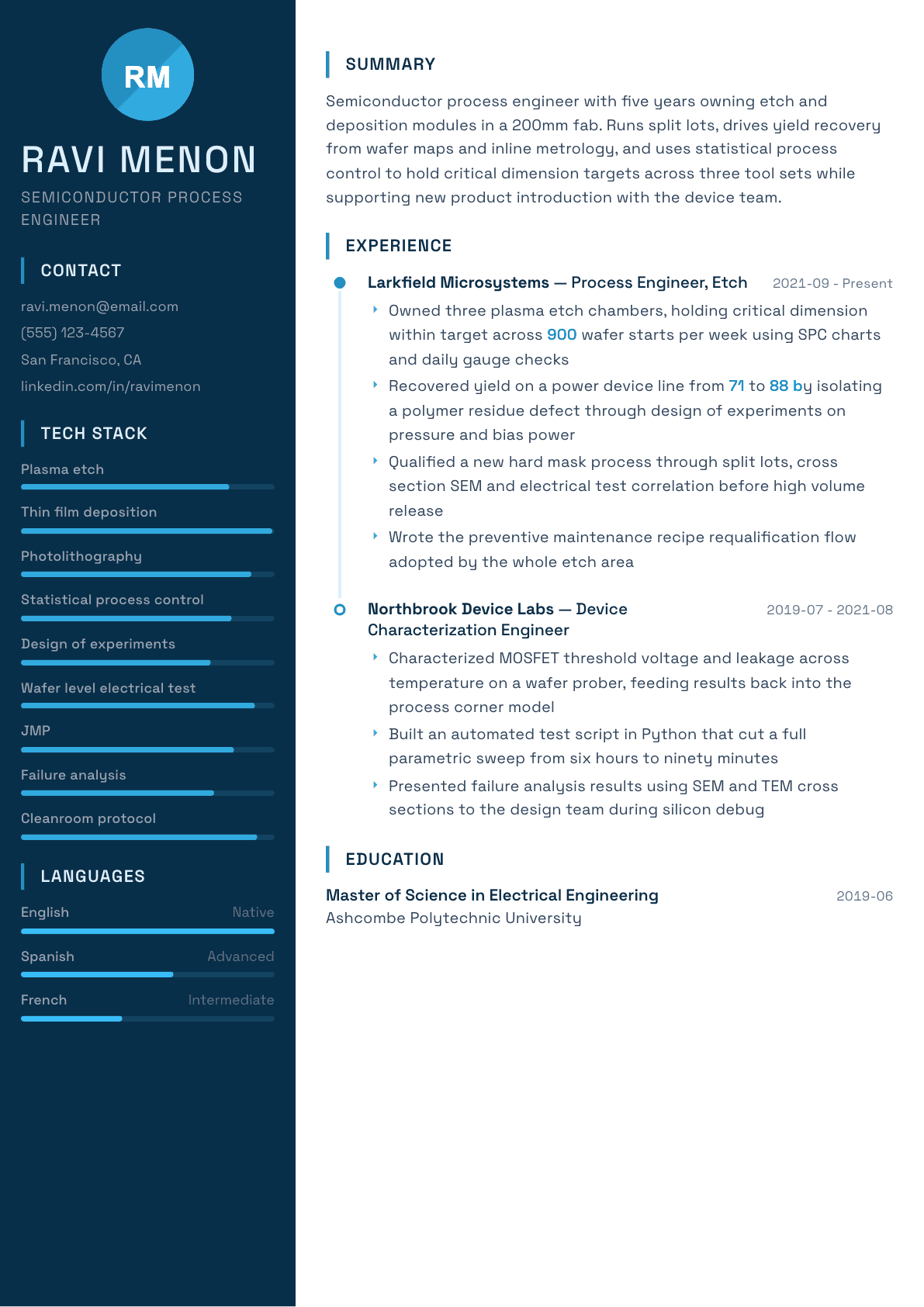
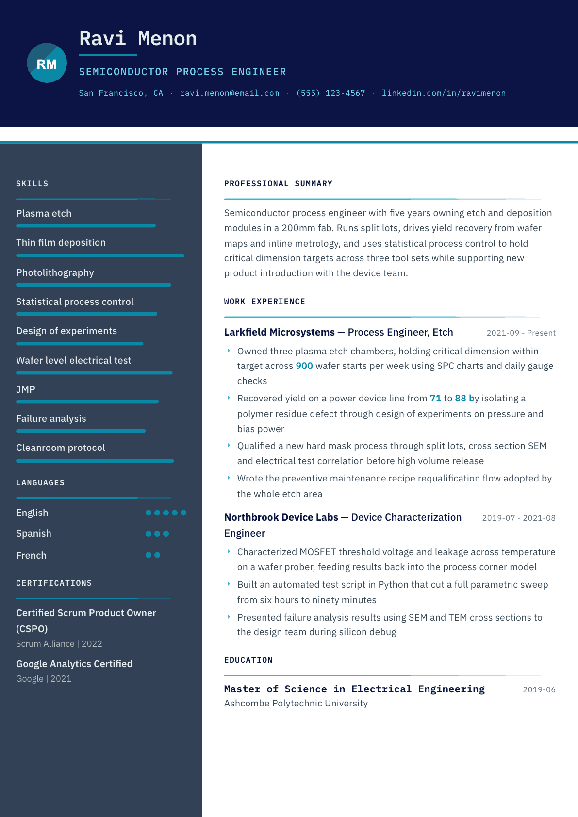
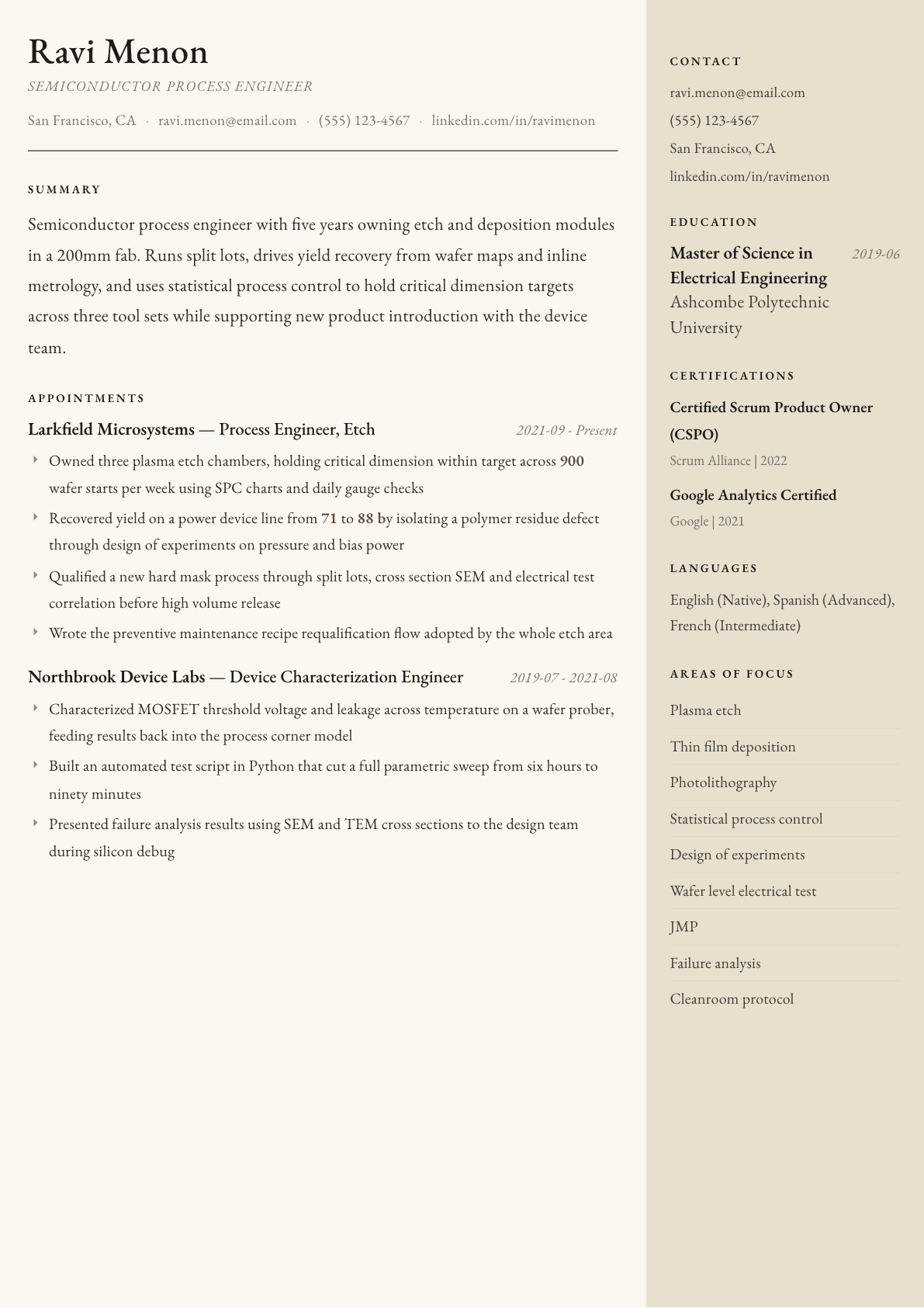
The same semiconductor engineer content laid out in three CVBooster templates, so you can see what the finished document looks like before you write a word.
Example Semiconductor Engineer summary
Semiconductor process engineer with five years owning plasma etch in a 200mm fab. Holds critical dimension inside target across three chambers using statistical process control, and recovers yield through design of experiments rather than guesswork. Raised line yield from seventy one to eighty eight by isolating a residue defect and requalifying the recipe. Master of Science in electrical engineering with device characterization and failure analysis experience.
Skills to list on a Semiconductor Engineer resume
- Plasma etch
- Chemical vapor deposition
- Photolithography
- Ion implantation
- Chemical mechanical planarization
- Statistical process control
- Design of experiments
- Yield analysis
- Wafer level electrical test
- Device characterization
- Failure analysis
- SEM and TEM cross sections
- JMP
- Python for test automation
- Cleanroom protocol
- New product introduction
What actually gets this resume read
- Name the process module you own, because fabs hire by module: etch, litho, diffusion, implant, CMP or thin films.
- State the wafer size and the technology node or device family you worked on, since that sets your credibility instantly.
- Quantify yield, defect density or critical dimension control, as these are the numbers a fab manager reads first.
- List the toolsets by maker where you can, along with the metrology and analysis software you actually use.
- Show statistical work explicitly: design of experiments, SPC limits, gauge studies and capability indices.
- Separate device characterization from process ownership so the reader can place you on the right side of the fab.
How to write a semiconductor engineer resume
Fabs hire by module. The manager reading your resume owns etch, or litho, or diffusion, or implant, or planarization, or thin films, and he is trying to work out in about fifteen seconds whether you have run tools and recipes in his area or in somebody else's. A semiconductor engineer resume that describes generic process engineering forces him to guess, and a guess in a hiring queue is a rejection.
The second thing he checks is whether you own numbers. Yield, defect density, critical dimension control, uniformity, tool availability and cycle time are the currency of a fab, and every one of them is measured continuously. If your resume has no numbers, the reader assumes you supported someone who did.
This guide covers how to declare your module and your wafer size, how to write yield and qualification bullets that survive a technical interview, where device characterization sits relative to process ownership, and the questions that come up when a fab engineer rewrites this document for a different node or a different company.
Format: single column, module named in the first line, two pages after a few years
Reverse chronological, plain layout, no side panels. Large semiconductor employers screen at volume and the parser sees your resume before any engineer does. Give the header your city and state, your phone, your email, and a title line that names the module rather than the generic job family.
Two pages is normal once you have owned tools. Use the second page for a technical block: toolsets, metrology, analysis software, and the process integration steps you have touched. Publications and patents get their own short block if you have them, with the title and the venue only.
- Header: name, city and state, phone, email, and the module you own.
- Sections in this order: summary, technical skills, experience, education, patents and publications.
- Recent graduates lead with education, then a research block naming the cleanroom tools they ran themselves.
Summary: module, wafer size, device family, and the metric you moved
Four lines. Name the module, the wafer size, the device family or technology generation, and one metric you personally improved. A semiconductor process engineer who writes plasma etch, 200mm, power devices, critical dimension control has told the reader more than three paragraphs of adjectives.
If you sit on the device side rather than the process side, say so and use the vocabulary of that job: threshold voltage, leakage, breakdown, corner models, silicon debug. Mixing the two vocabularies without a boundary makes both look shallow.
Experience: tools owned, splits run, yield recovered
Open each role with the environment: fab size, wafer size, device family, and how many chambers or tools you personally owned. Then write bullets around the four things a module engineer does. Sustaining, which is holding the process inside limits with control charts and gauge checks. Improvement, which is design of experiments and split lots. Qualification, which is bringing a new recipe, chamber or hard mask to release. And excursion response, which is finding the source of a yield hit and closing it.
Excursion bullets are the most valuable and the most often written badly. Name the signature you saw on the wafer map or the inline metrology, the hypothesis, the experiment that tested it, and the fix. A polymer residue traced through a pressure and bias power design of experiments is a story a reader can follow; improved yield is not.
Where you can, say what the process feeds and what it consumes. Etch engineers who understand the incoming litho profile and the downstream electrical result are the ones who get promoted, and one sentence proving that changes how the whole resume reads.
Statistics and tools: the vocabulary of a fab floor
A fab runs on statistics, so the resume should show them explicitly rather than implying them. Statistical process control limits, capability indices, gauge repeatability studies, design of experiments and response surface work all belong in bullets, attached to a decision you made with them. Name the analysis software you actually use, whether that is JMP, a scripted Python workflow, or the fab's own yield management system.
For toolsets, give the process and the maker where you are free to. For metrology, name what you read: scatterometry, critical dimension scanning electron microscopy, ellipsometry, four point probe, defect inspection and review. For failure analysis, say whether you request cross sections or interpret them yourself, because interpreting is the more valuable half.
- Module and chamber count you owned, with weekly wafer starts supported.
- Statistical methods with the decision each one drove.
- Metrology and inspection you read personally.
- Cleanroom protocol, gowning discipline and safety training for hazardous gases.
Keywords a semiconductor posting repeats
These postings are written from templates and reuse a narrow vocabulary: process module names, yield improvement, statistical process control, design of experiments, new product introduction, wafer acceptance test, root cause and corrective action, preventive maintenance and requalification. Mirror the wording once in the skills block and once inside a bullet where it is doing real work.
Avoid stuffing. An engineer reads the file immediately after the parser, and a keyword wall reads as someone with nothing specific to report.
Semiconductor Engineer resume summary examples
Recent graduate
Electrical engineering graduate with cleanroom research experience in plasma etch and thin film deposition on 100mm wafers. Ran split lots, measured film thickness by ellipsometry, and analyzed results in JMP. Seeking a process engineering position in an etch or deposition module.
Five years in
Semiconductor process engineer with five years owning plasma etch in a 200mm fab. Holds critical dimension inside target across three chambers using statistical process control, and recovered line yield from 71 to 88 on a power device by isolating a residue defect through a pressure and bias power study.
Module owner
Etch module owner with eleven years across power and analog device lines, responsible for recipe strategy, chamber matching and requalification standards for an entire process area. Leads new product introduction with integration and device teams, and mentors four engineers through excursion response and design of experiments.
Work experience bullets: before and after
Before: Responsible for etch process in the fab.
After: Owned three plasma etch chambers, holding critical dimension inside target across 900 wafer starts per week using control charts and a daily gauge check routine.
Chamber count, wafer volume and the control method show the scale and the discipline behind the ownership claim.
Before: Improved yield on a product line.
After: Recovered yield on a power device line from 71 to 88 by isolating a polymer residue defect through a design of experiments on chamber pressure and bias power, then locking the new window into the recipe.
The defect mechanism and the experiment turn a yield number into evidence that you found the cause yourself.
Before: Qualified a new process.
After: Qualified a new hard mask process through split lots, cross section imaging and electrical test correlation, then released it to high volume after a two week marathon run with no excursions.
Naming the qualification evidence shows a reader you can take a process from experiment to production release.
Before: Did device testing and reported results.
After: Characterized transistor threshold voltage and leakage across temperature on a wafer prober, feeding measured spread back into the process corner model used by the design team.
The measurement, the sweep condition and the downstream consumer make device work look like engineering rather than data collection.
Before: Automated some of the test work with scripts.
After: Wrote a Python test automation script that cut a full parametric sweep from six hours to ninety minutes and made overnight runs possible without an operator present.
The time saved and the operational change it enabled give the automation a value a manager can measure.
Hard skills
- Plasma etch
- Chemical vapor deposition
- Photolithography
- Ion implantation
- Chemical mechanical planarization
- Statistical process control
- Design of experiments
- Yield analysis and wafer mapping
- Wafer level electrical test
- Device characterization
- Failure analysis and cross section interpretation
- JMP
- Python for test automation
- Cleanroom protocol and hazardous gas safety
- New product introduction
Soft skills
- Excursion calm under production pressure
- Cross shift handoff discipline
- Working with integration and device teams
- Data first argument
- Documentation of recipe changes
Certifications worth listing
- Certified Quality Engineer (CQE) (American Society for Quality)
- Certified Six Sigma Green Belt (CSSGB) (American Society for Quality)
- Certified Reliability Engineer (CRE) (American Society for Quality)
Mistakes that cost semiconductor engineer candidates the interview
- Never naming the module, which leaves an etch manager and a litho manager both unsure whether the resume is for them.
- Omitting wafer size and device family, the two facts that place your experience in context faster than anything else.
- Reporting yield gains with no defect mechanism, which reads as team credit rather than personal work.
- Describing statistical tools as skills without ever showing a decision one of them drove.
- Blending device characterization and process ownership so neither background looks deep enough to hire.
- Listing every tool in the fab rather than the ones you personally qualified and requalified.
- Writing a keyword block so dense that the engineer reading after the parser cannot find a single real project.
Semiconductor Engineer resume questions
Should I name the technology node I worked on?
Name it if you are free to. Node or device generation is the fastest credibility signal in this field, and a reader uses it to judge how close your process control experience is to his. If a confidentiality agreement blocks it, give the device family and wafer size instead.
How do I write a semiconductor resume for a move from research to a production fab?
Lead with the tools you personally ran and the statistics you applied, not with your thesis topic. Production managers hire for hands on tool time, recipe discipline and the ability to work inside a control chart, so make each of those visible before any publication list.
Do patents and publications belong on a fab process resume?
Yes, but keep them short. A block with titles and venues at the end is enough for a process role. Only expand it if you are applying to a research or advanced development group, where the depth of the work is part of what is being evaluated.
How much yield detail can I safely include?
Describe the mechanism and the relative movement rather than absolute figures tied to a named product. Saying you took a line from the low seventies to the high eighties by fixing a residue defect communicates the achievement without exposing anything a former employer would consider confidential.
Is a Six Sigma certification useful for a process engineer?
It helps at the screening stage and it is common on manufacturing job descriptions, but it will never substitute for showing designed experiments in your bullets. Treat it as a supporting credential and let the experiments carry the technical argument.
Related resume examples
- Electrical Engineer Resume example
- Process Engineer Resume example
- Electronics Engineer Resume example
- Test Engineer Resume example
- R&D Engineer Resume example
- Metallurgical Engineer Resume example